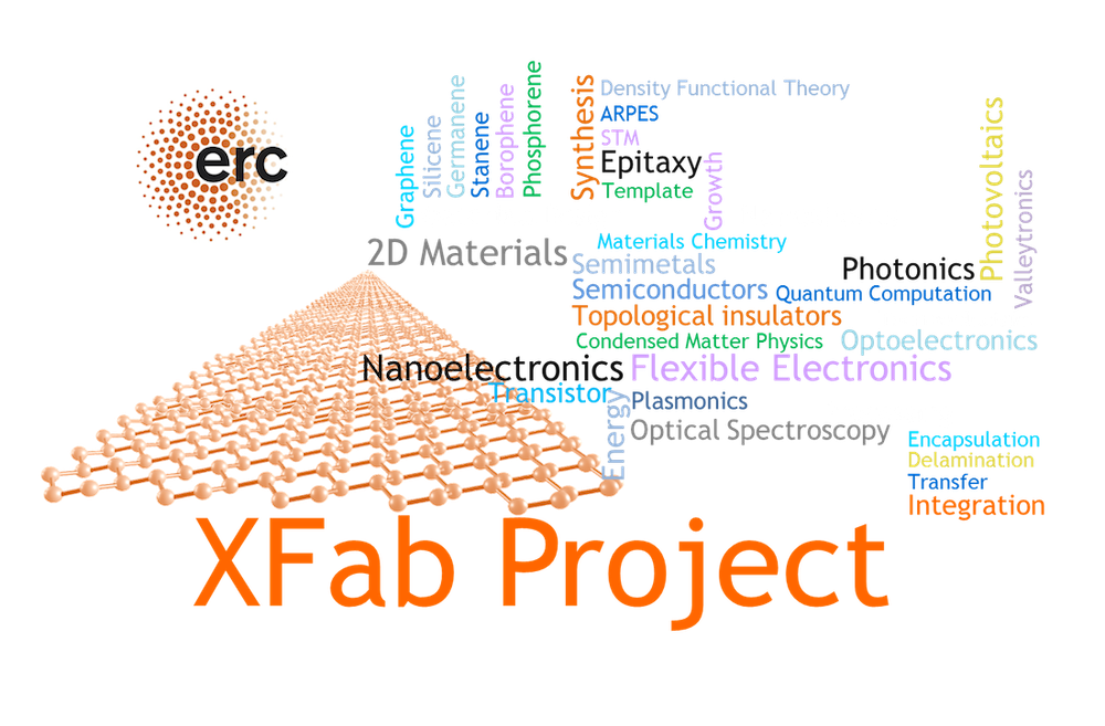
The @XFab Project arises from an ERC CoG 2017 grant to @AlessandroMolle. X points to the kind of atoms that consititute the epitaxial #Xenes, an emerging class of monoelemental 2D-materials beyond graphene (silicene, germanene, stanene, etc.). Fab means production, process standardization, and device integration of the Xenes. The XFab scope is to develop new manufacturing paths for a Xene-based nanotechnology spanning from nanoelectronics to photonics and more.
Contact: Alessandro Molle
Website by Roberto Colnaghi
Website by Roberto Colnaghi
Research
Research
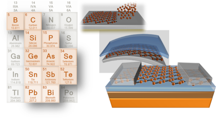
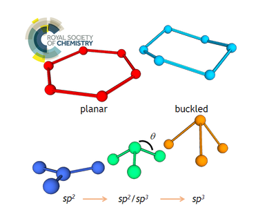
The Xene stage 2D monoelemental crystals beyond graphene are an emerging branch that ranges from exfoliable flakes of phosphorene to epitaxial 2D lattices on substrate such as silicene. The latter subclass is usually referred to as Xenes with X initially denoting the group IVA semiconductors (Si, Ge, and Sn resulting in silicene, germanene, and stanene, respectively) and recently being extended to some elements in the group IIIA (e.g. B), VA (P,As,Sb,Bi), and VIA (Se,Te) of the Mendeleev table. Different from graphene, #Xenes are epitaxially grown crystals with a buckled lattice structure. Epitaxy is the path through which the Xenes are grown on suitable templates.
Research
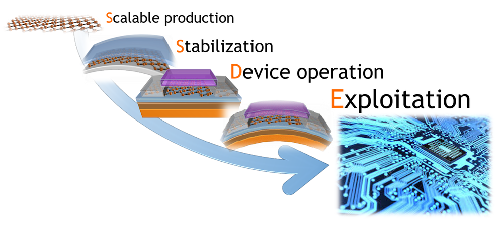
Production schemes The @XFab Project aims to create a portfolio of stabilized Xenes and Xene-related materials suitable for device integration by releasing protocols for the growth, post-growth processing, and stabilization. A prototypical example of it is the case of the encapsulated silicene supported by mica substrates. These production schemes are intended to define a quality standard for Xenes to be implemented in device structures (e.g. transistors), and thus bring the current lab research level to a technology proven in lab.
Research
Xene devices The @XFab Project aims at the verification of the electrical output of processable Xenes when integrated into a device structure. A paradigmatic example of it is the case of the silicene transistors including silicene single- and multi-layer by delamination, and silicene-based heterosheets. Devices for this purpose will include diode and triode structures (e.g. junctions and transistor), as well as plasmonic structures.
As for graphene, a question remains as to what impact Xene may have on the scientific community as well as on societal challenges. A portfolio of fully exploitable materials (namely from the synthesis to the handable material package) is the direction of the XFab project to address the broadest range of application targets.
As for graphene, a question remains as to what impact Xene may have on the scientific community as well as on societal challenges. A portfolio of fully exploitable materials (namely from the synthesis to the handable material package) is the direction of the XFab project to address the broadest range of application targets.
Goals
Goals
Fill the gap The number of synthetic Xenes is nowadays tremendously expanding and so is their potential in applications (see here). Some of them may work for logic or analogic electronic devices with benefit on the power consumption; some are suitable for topological matters (quantum spin Hall insulators) or as intrinsically anisotropic materials. Overall, a viable technology integration path is still missing, and fulfil this gap is the key enabling step for a Xene to have an impact on applications targets (nanoelectronics, photonics, energy, etc.) as well as societal challenges (internet of things, internet of everything, smart living, etc.)
Goals
Put the pieces together Nowadays, Xenes are a puzzle of different materials. Some Xenes are produced as nanoscale pieces, The XFab objective is reassemble the Xene puzzle in a unitary framework where only the Xenes that can bear a viable application will be selected. Requisites are large-scale synthesis and atomically-resolved identification.
Goals
One step closer to the device Field-effect transistor is the flag-vehicle to disclose the Xene ID. But it is not the only technology enabler. Xenes can be reduced to junctions or other gated structures for energy and photonics applications as well. Main bottlenecks are the stabilization and handling from the pristine form of epitaxial 2D lattices. Xene integration into operational devices will be a key-target.
People
Open positions
Take a look at the CNR-IMM job opportunities @Agrate
Contact Alessandro Molle for further information.
Alessandro Molle
[PI] Born in 1977, MSc (Physics) and PhD (Materials Science) from the University of Genoa, he is the PI of the XFab Project as a winner of the ERC-COG 2017 grant, and a senior researcher at the CNR-IMM, unit of Agrate Brianza. From 2011, mostly involved in unconventional 2D materials like the Xenes, or scalable production schemes for 2D transition metal dichalcogenides. Mind-tailored for nanoelectronic applications (logics and memories), but currently concerned with exploitation of 2D materials in photonics and other technology fields. Technically specialized in nanomaterials synthesis (MBE, CVD) and advanced characterization. Co-editor of a CRC book about 2D materials for nanoelectronics in 2016. Connected to STMicroelectronics-Agrate for a Research Contract and to UniMib for PhD course teaching. More on Scholar or ORCID Follow me on Twitter: @AlessandroMolle Contact: alessandro.molle@cnr.it, Skype ID: alessandro_molle
[PI] Born in 1977, MSc (Physics) and PhD (Materials Science) from the University of Genoa, he is the PI of the XFab Project as a winner of the ERC-COG 2017 grant, and a senior researcher at the CNR-IMM, unit of Agrate Brianza. From 2011, mostly involved in unconventional 2D materials like the Xenes, or scalable production schemes for 2D transition metal dichalcogenides. Mind-tailored for nanoelectronic applications (logics and memories), but currently concerned with exploitation of 2D materials in photonics and other technology fields. Technically specialized in nanomaterials synthesis (MBE, CVD) and advanced characterization. Co-editor of a CRC book about 2D materials for nanoelectronics in 2016. Connected to STMicroelectronics-Agrate for a Research Contract and to UniMib for PhD course teaching. More on Scholar or ORCID Follow me on Twitter: @AlessandroMolle Contact: alessandro.molle@cnr.it, Skype ID: alessandro_molle
People

Carlo Grazianetti
[key-investigator] earned Ph.D. from University of Milano-Bicocca in 2014 defending a thesis on the scanning tunneling microscopy investigation of III-V semiconductors and new 2D nanolattices. Currently post-doc fellow at CNR-IMM unit of Agrate Brianza. Since 2011, key-investigator of molecular beam epitaxy and scanning probe microscopy tasks in EU projects on the synthesis and integration of Xenes into devices.
More on Scholar or ORCID
Follow me on Twitter @CGrazianetti
Contact: carlo.grazianetti@mdm.imm.cnr.it
People

Christian Martella
[key-investigator] graduated in Physics in 2009 from the University of Pisa and he earned his Ph.D in Nanotechnology in 2013 from the University of Genoa. Focused on the study of light-matter interaction at the nanoscale in plasmonic and dielectric structures. In 2015, he joined the 2D-material group at CNR-IMM unit of Agrate-Brianza unit working on the growth and characterization of transition metal dichalcogenides.
More on Scholar or ORCID.
Contact: christian.martella@mdm.imm.cnr.it
People
Alessio Lamperti
[key-investigator] M.Eng.(Nuclear Engineering) and Ph.D. (Radiation Science and Technology) at Politecnico di Milano is research engineer at CNR-IMM. Expert in advanced structural and physical-chemical characterization of superlattices, thin films, layers and 2D nanosheets (MoS2) by means of X-Ray scattering techniques (XRR, GIXRD) and analytical methods (XPS, FT-IR, Raman Spectroscopy, ToF-SIMS). Connected to STMicroelectronics-Agrate for a Research Contract and to PoliMi for seminars in PhD courses.
More on Scholar or ORCID.
Contact: alessio.lamperti@cnr.it
Skype ID: alex_ba3709
People

Gabriele Faraone
[PhD] got his MSc in Physics in 2017 from University of Milano. PhD student in Material Science and Nanotechnology at Università of Milano-Bicocca with Prof. Emiliano Bonera and Dr. Alessandro Molle. He joined to the 2D-Material Group at CNR-IMM unit of Agrate Brianza on the project focused on Phosphorene and Silicene.
Contact: gabriele.faraone@mdm.imm.cnr.it
People
Collaborators
Prof. Deji Akinwande, University of Texas at Austin
Prof. Stefano Lupi, University of Rome “La Sapienza”
Prof. Emiliano Bonera, University of Milan Bicocca
Prof. Olivia Pulci, University of Rome Tor Vergata
Prof. Deji Akinwande, University of Texas at Austin
Prof. Stefano Lupi, University of Rome “La Sapienza”
Prof. Emiliano Bonera, University of Milan Bicocca
Prof. Olivia Pulci, University of Rome Tor Vergata
Products
Spotlight
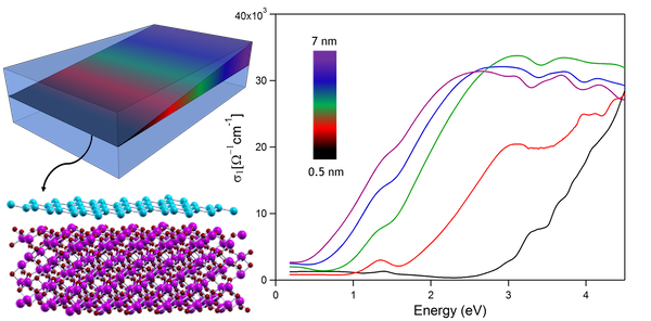
C. Grazianetti, S. La Rosa, C. Martella, P. Targa, D. Codegoni, P. gori, O. Pulci, A. Molle*, and S. Lupi*, "Optical Conductivity of Two-Dimensional Silicon: Evidence of Dirac Electrodynamics"
Products
Spotlight
A. Molle, C. Grazianetti*, L. Tao*, D. Taneja, Md. Hasibul Halam, and D. Akiwande*, "Silicene, silicene derivatives, and their device applications"
Products
Past Stories
Silicene Goes Multilayer! How to make a silicene multilayer starting from a single layer and integrate it in an ambipolar and air-stable transistor. Look at: C. Grazianetti, E. Cinquanta, L. Tao, P. De Padova, C. Quaresima, C. Ottaviani, D. Akinwande, and A. Molle, "Silicon Nanosheets: Crossover between Multilayer Silicene and Diamond-like Growth Regime" ACS Nano 11, 3376 (2017), DOI: 10.1021/acsnano.7b00762
A perspective on two-dimensional Xenes: whether emerging Xenes may a chance in future nanoscience and nanotechnology. Look at: A. Molle, J. Goldberger, M. Houssa, Y. Xu, S.-C. Zhang, and D. Akinwande, "Buckled two-dimensional Xene sheets", Nature Materials, 16, 163 (2017) DOI: 10.1038/NMAT4802 (2017)
The silicene transistor: the very first case of silicene single layer integration into a field effect transistor. Look at: L. Tao, E. Cinquanta, D. Chiappe, C. Grazianetti, M. Fanciulli, M. Dubey, A. Molle, and D. Akinwande, "Silicene field-effect-transistors operating at room temperature" Nature Nanotechnology 10, 227 (2015), doi:10.1038/nnano.2014.325
Silicene encapsulation: How to make air-reactive silicene-on-silver stable in the environment. Look at: 34. A. Molle*, C. Grazianetti, D. Chiappe, E. Cinquanta, E. Cianci, G. Tallarida, and M. Fanciulli, “Hindering the Oxidation of Silicene with Non-Reactive Encapsulation”, Adv. Funct. Mater. 23, 4340 (2013)
Multiphase silicene: not only one silicene, but a number of buckled phases! Look at: 38. D. Chiappe, C. Grazianetti, G. Tallarida, M. Fanciulli, and A. Molle*, “Local electronic properties of corrugated silicene phases”, Adv. Mater. 24, 5088 (2012)
Products
Confs, Workshops, and Schools
Jun 2019: Alessandro doubly invited at the E-MRS 2019 Spring Symps D and T @Nice
Apr 2019: Alessandro invited at the MRS 2019 Spring QN03 @Phoenix
Feb 2019: Gabriele visiting Deji’s group at the Univ Texas @Austin
Jan 2019: Carlo on the way of the N2D 2019 conf (Shanghai)
Oct 2018: New invited seminar for Alessandro at Materials.it 2018 (Bologna)
Sept 2018: Alessandro towards Italy-Canada Bilateral Workshop (Montréal) & Nanoinnovation 2018 (Rome) and Carlo invited talk at SIF 2018
Jul 2018: Alessandro and Gabriele at Erice School! Invited seminar for Alessandro at the #Epioptics-15 and #2DNano workshop